(China (Mainland))

Product Summary
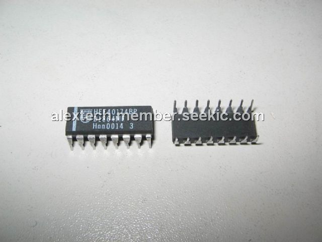
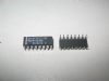
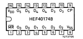
The HEF40174BP is a hex edge-triggered D-type flip-flop with six data inputs (D0 to D5), a clock input (CP), an overriding asynchronous master reset input (MR), and six buffered outputs (O0 to O5). Information on D0 to D5 is transferred to O0 to O5 on the LOW to HIGH transition of CP if MR is HIGH. When LOW, MR resets all flip-flops (O0 to O5 = LOW) independent of CP and D0 to D5.
Parametrics
HEF40174BP absolute maximum ratings: (1)VDD supply voltage: -0.5 to +18 V; (2)IIK input clamping current VI < -0.5 V or VI > VDD + 0.5 V: ±10 mA; (3)VI input voltage: -0.5 to VDD + 0.5 V; (4)IOK output clamping current VO < -0.5 V or VO > VDD + 0.5 V: ±10 mA; (5)II/O input/output current: 10 mA; (6)IDD supply current: 50 mA; (7)Tstg storage temperature: -65 to +150 ℃; (8)Tamb ambient temperature: -40 to+85 ℃; (9)Ptot total power dissipation DIP16 package: 750 mW; (10)SO16 package: 500 mW; (11)P power dissipation per output: 100 mW.
Features
HEF40174BP features: (1)Propagation delays: 75 to 155 ns; (2)LOW to HIGH: 75 to 155 ns; (3)HIGH to LOW: 85 to 175 ns; (4)Output transition times: 60 to 120 ns; (5)Set-up time: 20 to 10 ns; (6)Hold time: 10 to 0 ns; (7)Minimum clock pulse width: 70 to 35 ns; (8)Recovery time for MR: 45 to 25 ns; (9)Maximum clock pulse frequency: 5 to 11 MHz.
Diagrams
| Image | Part No | Mfg | Description |  |
Pricing (USD) |
Quantity | ||||||||||||
|---|---|---|---|---|---|---|---|---|---|---|---|---|---|---|---|---|---|---|
 |
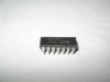
 HEF40174BP,652 |
NXP Semiconductors |
Flip Flops HEX D-TYPE FLIP-FLOP |
Data Sheet |
|
|
||||||||||||
|
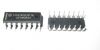
HEF40174BPN |
NXP Semiconductors |
Flip Flops HEX D-TYPE FLIP-FLOP |
Data Sheet |
Negotiable |
|
||||||||||||