Product Summary
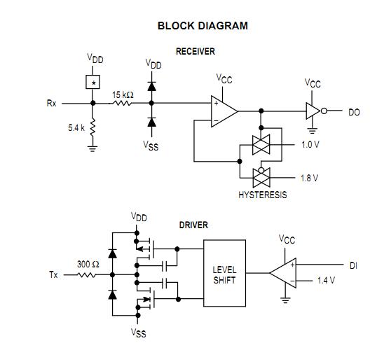
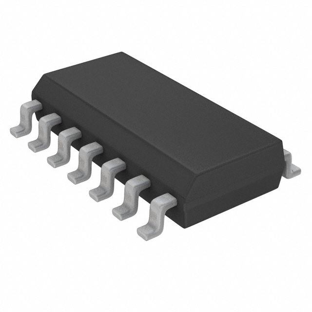
The MC145406DW is a silicon–gate CMOS IC that combines three drivers and three receivers to fulfill the electrical specifications of standards EIA 232–E and CCITT V.28. The MC145406DW feature true TTL input compatibility, slew–rate–limited output, power–off source impedance, and output typically switching to within 25% of the supply rails. The MC145406DW can handle up to ± 25 V while presenting 3 to 7 kΩ impedance. Hysteresis in the receivers aids reception of noisy signals. By combining both drivers and receivers in a single CMOS chip, the MC145406DW provides efficient, low–power solutions for EIA 232–E and V.28 applications.
Parametrics
MC145406DW absolute maximum ratings: (1)DC Supply Voltages (VDD ≥ VCC) VDD: – 0.5 to + 13.5V; VSS: + 0.5 to – 13.5V; VCC:– 0.5 to + 6.0V; (2)Input Voltage Range, Rx1–3 Inputs, VIR: (VSS – 15) to (VDD + 15)V; DI1–3 Inputs:– 0.5 to (VCC + 0.5)V; (3)DC Current Per Pin: ± 100 mA; (4)Power Dissipation, PD: 1.0 W; (5)Operating Temperature Range, TA: – 40 to + 85℃; (6)Storage Temperature Rate, Tstg: – 85 to + 150℃.
Features
MC145406DW features: (1)± 5 V to ±12 V Supply Range; (2)300–Ω Power–Off Source Impedance; (3)Output Current Limiting; (4)TTL Compatible; (5)Maximum Slew Rate = 30 V/μs; (6)± 25 V Input Voltage Range When VDD = 12 V, VSS = – 12 V; (7)3 to 7 kΩ Input Impedance; (8)Hysteresis on Input Switchpoint.
Diagrams

 |
 MC14000UB |
 Other |
 |
 Data Sheet |
 Negotiable |
|
||||||||||||||||
 |
 MC14001B |
 Other |
 |
 Data Sheet |
 Negotiable |
|
||||||||||||||||
 |
 MC14001BCP |
 ON Semiconductor |
 IC GATE NOR QUAD CMOS 14DIP |
 Data Sheet |

|
|
||||||||||||||||
 |
 MC14001BCPG |
 ON Semiconductor |
 Gates (AND / NAND / OR / NOR) 3-18V Quad 2-Input NOR |
 Data Sheet |

|
|
||||||||||||||||
 |
 MC14001BDG |
 ON Semiconductor |
 Gates (AND / NAND / OR / NOR) 3-18V Quad 2-Input NOR |
 Data Sheet |

|
|
||||||||||||||||
 |
 MC14001BDR2 |
 |
 IC GATE NOR QUAD CMOS 14SOIC |
 Data Sheet |

|
|
||||||||||||||||
 (China (Mainland))


